Overview
Our group uses transmission electron microscopy and electron energy loss spectroscopy to understand nanomaterials and devices at the atomic scale. Using recent advances in aberration-corrected electron microscopy, we aim to image the structure, bonding, electronic, optical properties of materials with unprecedented precision. Together, this research aims to harness the incredible insights of atom-by-atom microscopy to design novel nanomaterials and devices.
Advanced electron microscopy methods
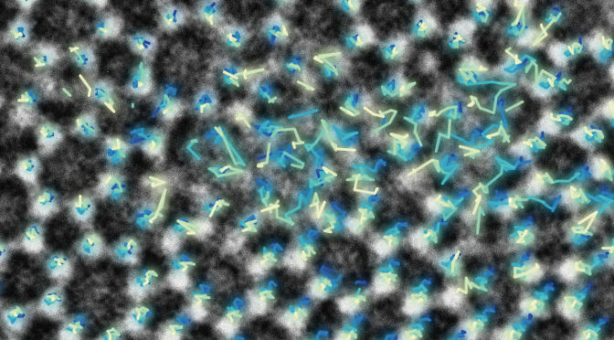
How do we push electron microscopy beyond generating “pretty pictures” to extract structural, chemical, and dynamic behavior of materials with single atom precision? Our group develops new microscopy techniques, such as 4D Scanning Transmission Electron Microscopy, electron ptychography, and electron spectroscopy. To interpret these data, we often reach across disciplines to borrow techniques from machine learning, biological imaging, and computer vision to develop new algorithms for processing electron microscopy and spectroscopy data. We have used these algorithms to reconstruct the 3D structure of materials a single layer thick, pick out and measure the statistical distributions of single dopants, and track each atom in a glass as it bends and breaks.
Nanoelectronics and nanophotonics
Low-dimensional materials such as atomic layers of graphene, molybdenum disulfide, black phosphorous, and tungsten ditelluride are leading to new designs for high-mobility, high-efficiency nanoelectronic and nanophotonic devices. In these systems, control at the single atom level is critical because defects, dopants, and interfaces have dramatic effects on the properties of materials only few atoms thick. 2D materials can be strongly tuned through defect or interfacial engineering to create and pattern atomically-thin circuitry, engineer low-power phase change memories, and produce high-efficiency absorbers and emitters of light. We use electron microscopy and spectroscopy, paired with advanced methods in computation and data processing, to probe the quantum phenomena that originate from individual atomic-scale defects and interfaces. By correlating atom-by-atom imaging and spectroscopy with in- and ex-situ device measurements, we can trace a direct link between atomic structure and chemistry, microstructure, and device performance. Examples of the impact of our work include: new designs for scalable, high-mobility graphene devices and 2D heterostructures with atomically precise interfaces.